FDMS3606AS
FDMS3606AS is Asymmetric Dual N-Channel MOSFET manufactured by onsemi.
Features
Q1: N-Channel
- Max r DS(on) = 8 mΩ at VGS = 10 V, ID = 13 A
- Max r DS(on) = 11 mΩ at VGS = 4.5 V, ID = 11 A Q2: N-Channel
- Max r DS(on) = 1.9 mΩ at VGS = 10 V, ID = 27 A
- Max r DS(on) = 2.8 mΩ at VGS = 4.5 V, ID = 23 A
- Low inductance packaging shortens rise/fall times, resulting in lower switching losses
- MOSFET integration enables optimum layout for lower circuit inductance and reduced switch node ringing
- Ro HS pliant
General Description
This device includes two specialized N-Channel MOSFETs in a dual PQFN package. The switch node has been internally connected to enable easy placement and routing of synchronous buck converters. The control MOSFET (Q1) and synchronous Sync FET (Q2) have been designed to provide optimal power efficiency.
Applications
- puting
- munications
- General Purpose Point of Load
- Notebook VCORE
- Sever
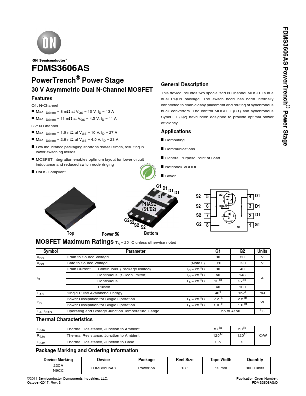
G1 D1 D1 D1 D1
PHASE (S1/D2)
G2S2S2 S2
Top
Power 56
Bottom
MOSFET Maximum Ratings TA = 25 °C unless otherwise noted
Symbol VDS VGS
EAS PD TJ, TSTG
Parameter Drain to Source Voltage Gate to Source Voltage Drain Current -Continuous (Package limited)
-Continuous (Silicon limited) -Continuous -Pulsed Single Pulse Avalanche Energy Power Dissipation for Single Operation Power Dissipation for Single Operation Operating and Storage Junction Temperature Range
Thermal Characteristics
RθJA RθJA RθJC
Thermal Resistance, Junction to Ambient Thermal Resistance, Junction to Ambient Thermal Resistance, Junction to Case
Package Marking and Ordering Information
S2 5 S2 6 S2 7 G2 8
Q2
4 D1
PHASE
3 D1 2 D1
Q1
1...