Datasheet Details
- Part number
- CY7C1371C
- Manufacturer
- Cypress
- File Size
- 791.68 KB
- Datasheet
- CY7C1371C_Cypress.pdf
- Description
- 18-Mbit (512K x 36/1M x 18) Flow-Through SRAM with NoBL Architecture
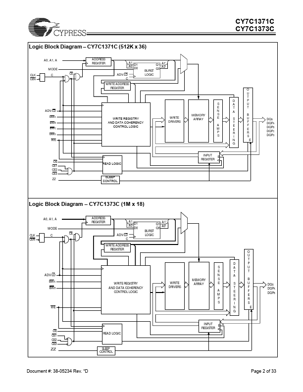
CY7C1371C Description
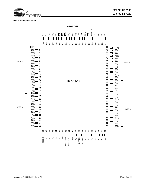
CY7C1371C CY7C1373C 18-Mbit (512K x 36/1M x 18) Flow-Through SRAM with NoBL™ Architecture .
1]
The CY7C1371C/CY7C1373C is a 3.
CY7C1371C Features
* No Bus Latency™ (NoBL™) architecture eliminates dead cycles between write and read cycles
* Can support up to 133-MHz bus operations with zero wait states
* Data is transferred on every clock
* Pin compatible and functionally equivalent to ZBT™ devices
* Int
📁 Related Datasheet
📌 All Tags
CY7C1371C Stock/Price