Datasheet Details
| Part number | FDT86113LZ |
|---|---|
| Manufacturer | ON Semiconductor |
| File Size | 269.43 KB |
| Description | N-Channel MOSFET |
| Datasheet |
 FDT86113LZ Datasheet FDT86113LZ Datasheet
|
|
|
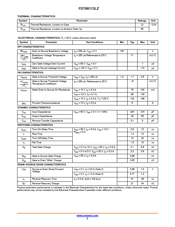
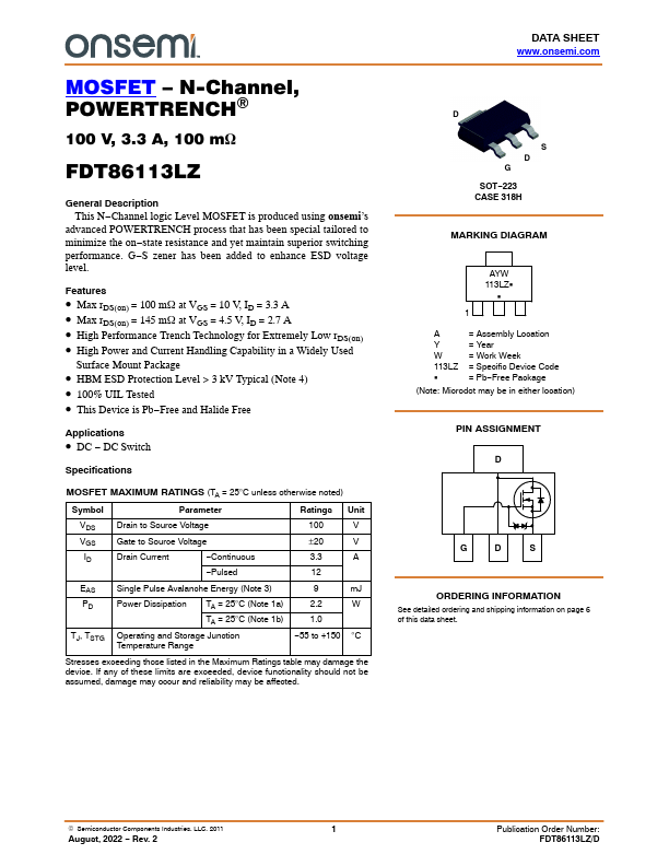
state resistance and yet maintain superior switching performance.
S zener has been added to enhance ESD voltage level.
| Part number | FDT86113LZ |
|---|---|
| Manufacturer | ON Semiconductor |
| File Size | 269.43 KB |
| Description | N-Channel MOSFET |
| Datasheet |
FDT86113LZ Datasheet
|
|
|
|